This is continued from my previous post about using Inkscape to draw pcb and front panel designs. When I last left you, I had created a multi-layered inkscape drawing that had front and back designs for the PCB along with a drill pattern for the panel.
First I'm going to get out my Toner Transfer paper. This is thick stock paper with a water soluble coating. It allows you to fuse a printed image to a surface and then remove the paper when submerged in water. The stuff is a little pricey at about $1 a page, but it's well worth it for making good clean transfers.
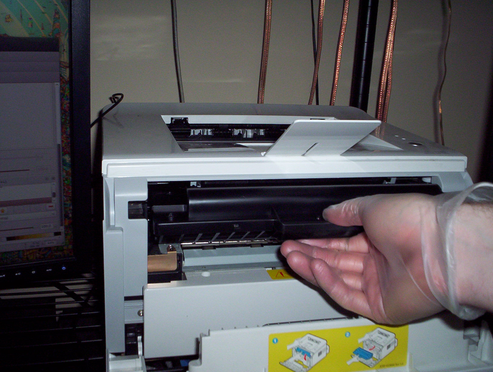
I'm using my home laser printer to make the PCB transfer. Ink from a laser printer is fused to the paper when heat and pressure is applied. Note that an inkjet printer uses a different method not suitable for the process I'm describing here. LASER PRINTERS ONLY. I keep a spare laser printer cartridge that I use solely for making PCBs. It's best to have a dark layer of ink. Regular printing jobs will run down the cartridge and I do this often enough that it makes sense to have a separate cartidge.
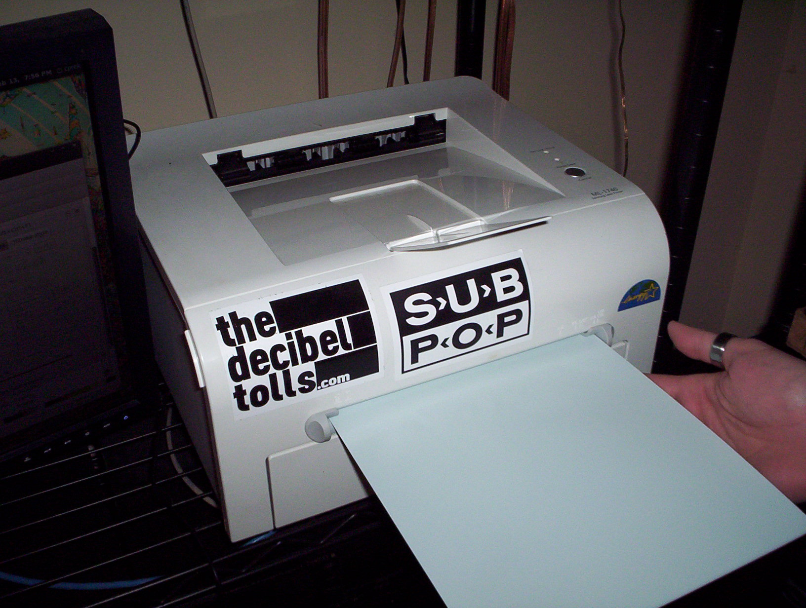
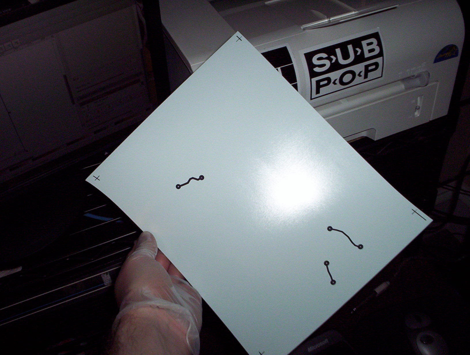
I start the print job and manually feed the Toner Transfer paper. Make sure you're printing on the shiny reflective side!
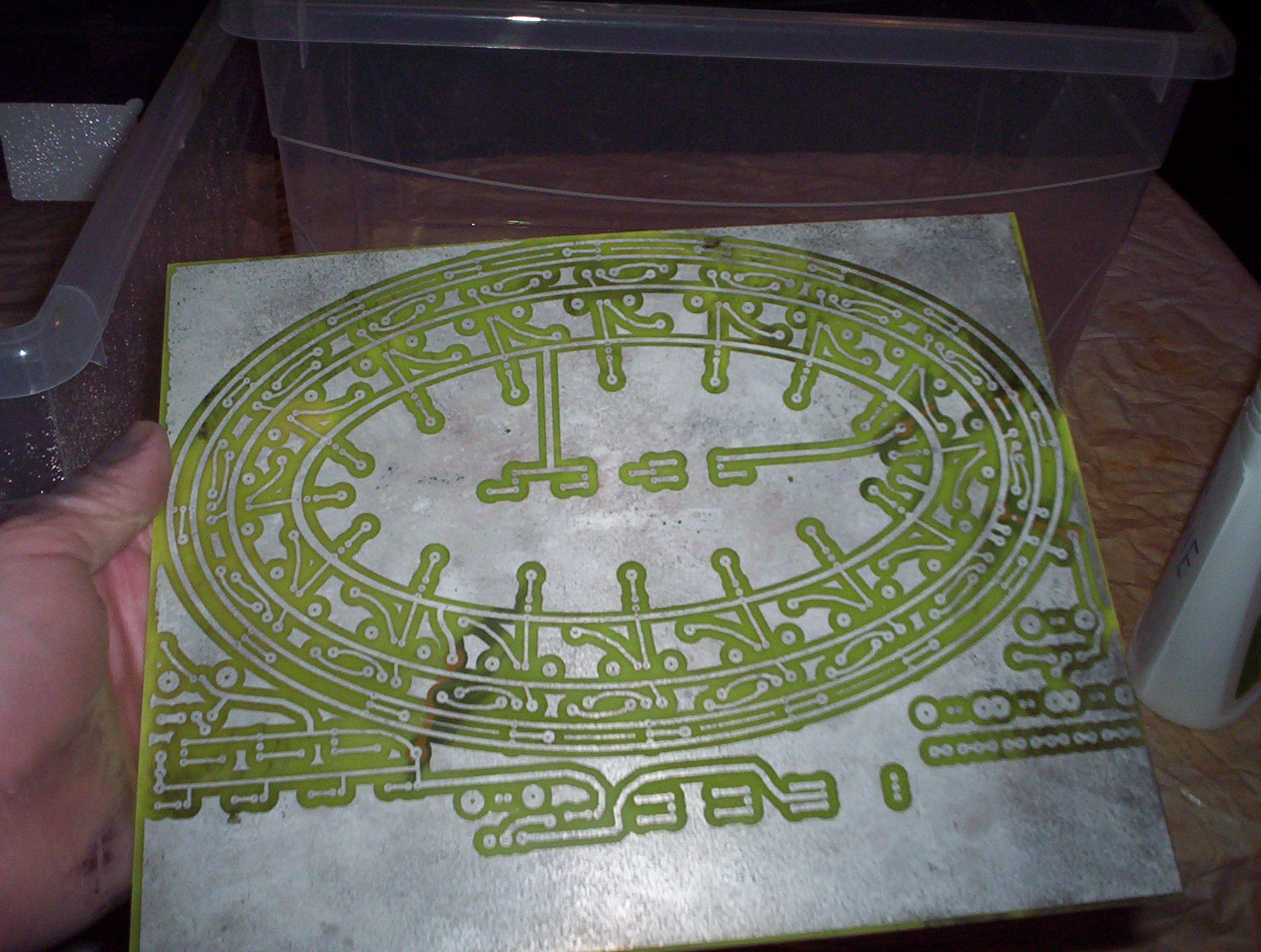
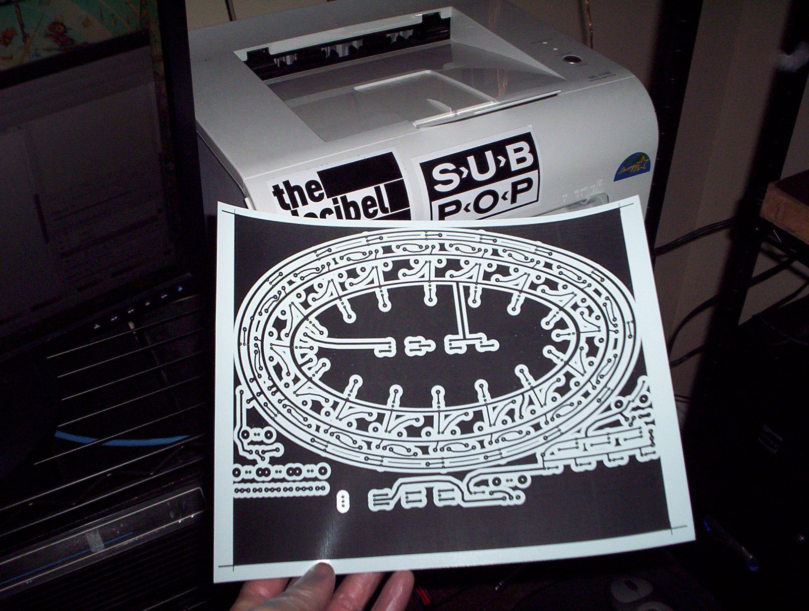
The print out looks good! Notice that I added a mask to the original drawing to darken up areas not in use. This makes the paper adhere better in the heat transfer process and also means you don't need to use as much etchant during the etching process to unnecessarily remove copper that's not being used for anything.
Did I mention this board is double-sided? Here I took the top copper layer from inkscape and flipped the image horizontally so it'll match up. Be careful when rendering your PCB traces for transfer... When you do a transfer of the image to a surface it's a mirror image. It's always good to do a test print on regular paper first for a sanity check to make sure you have it correct.
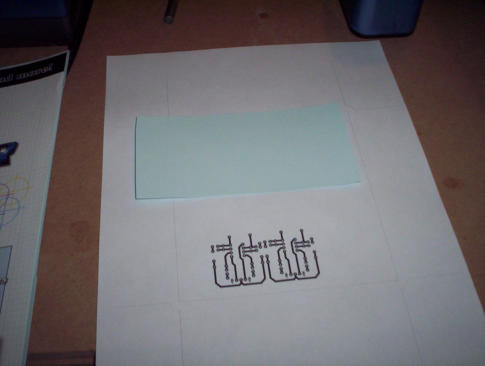
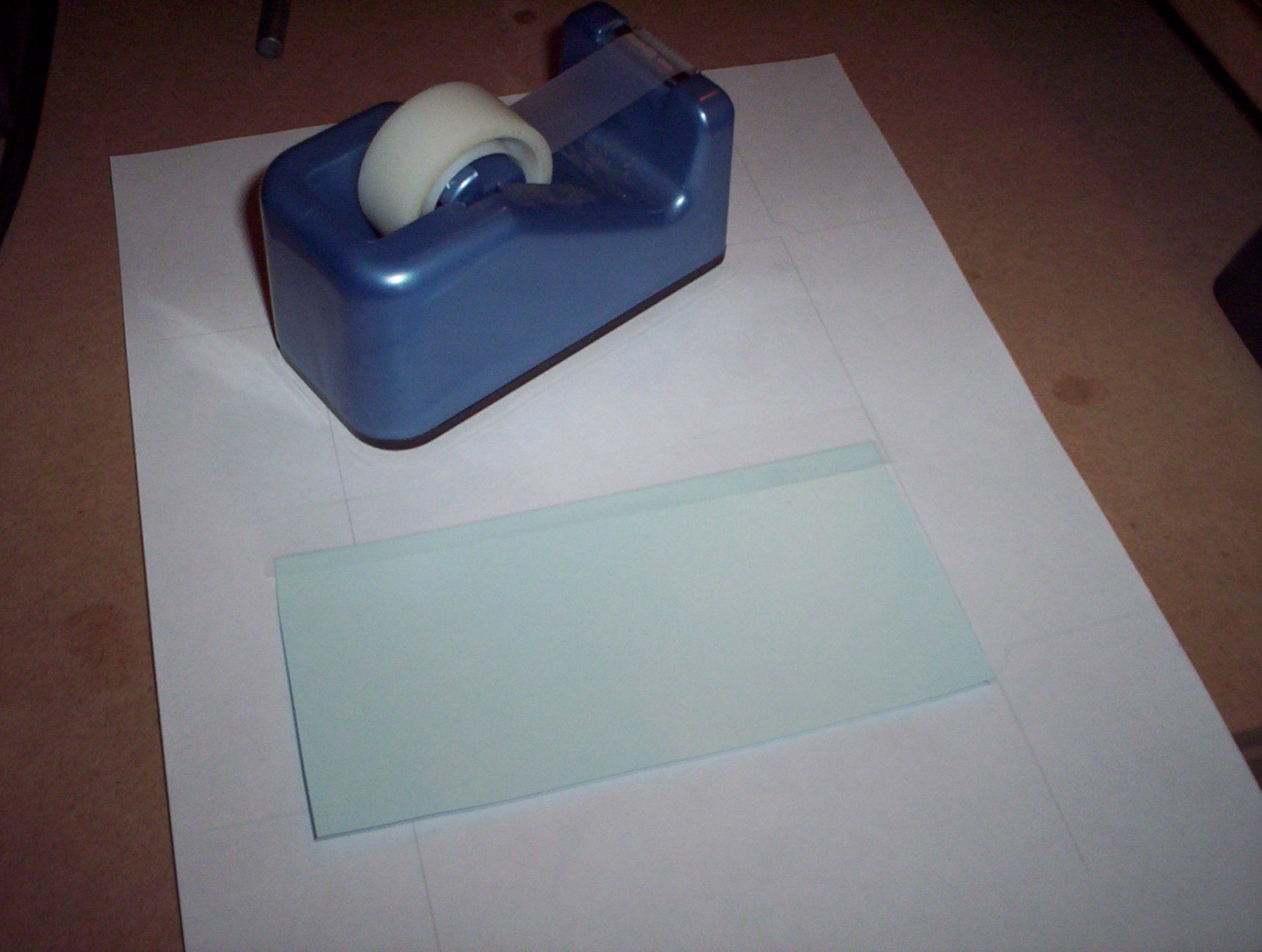
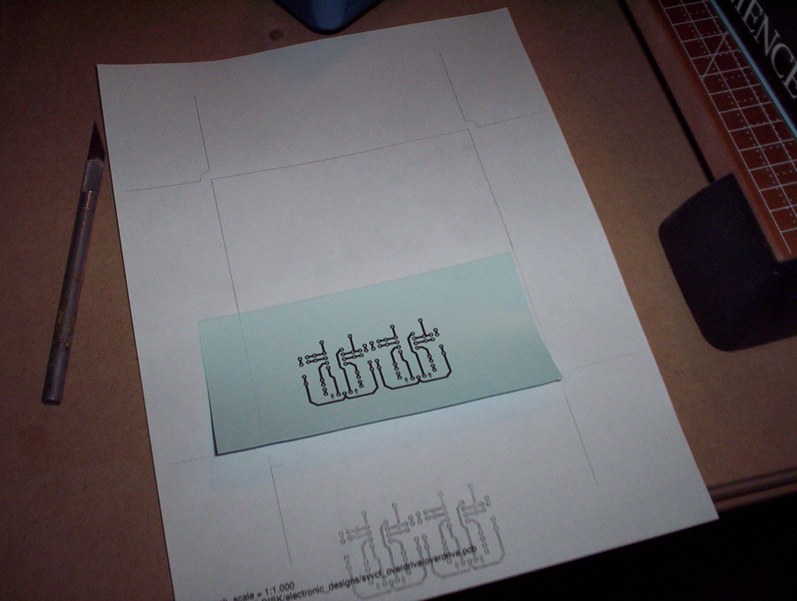
Since I'm getting out all the chemicals, I'm also making a PCB for a VCF overdrive I designed. Because toner transfer paper is fairly expensive I keep unused scraps for smaller PCBs. You can tape it to a regular piece of paper to print on the small scrap. In other words, use every part of the buffalo.
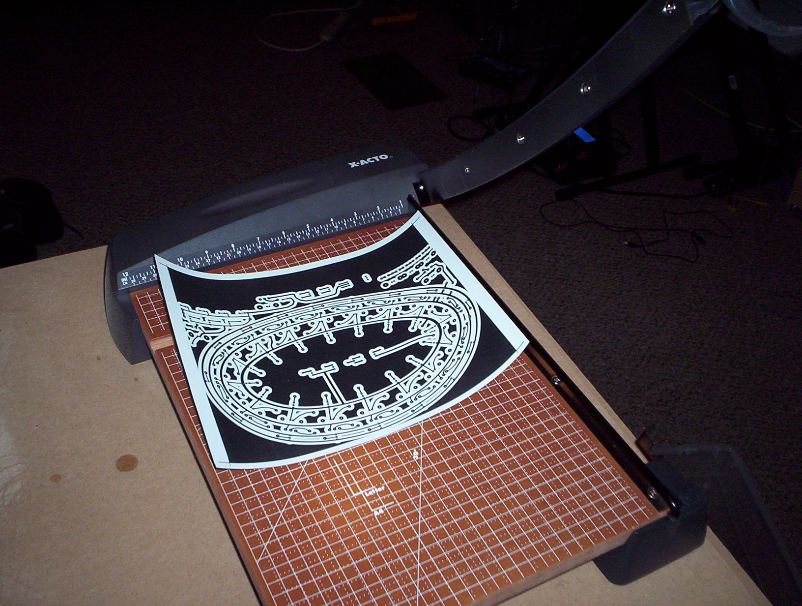
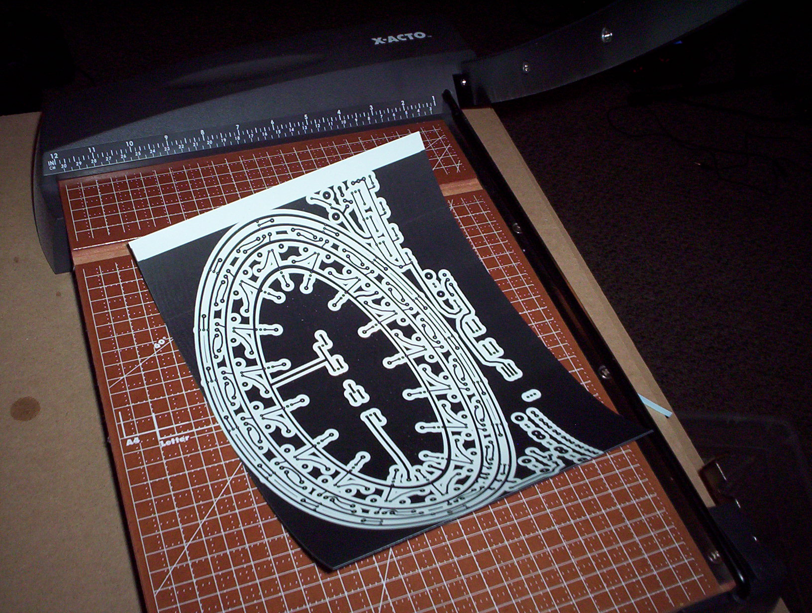
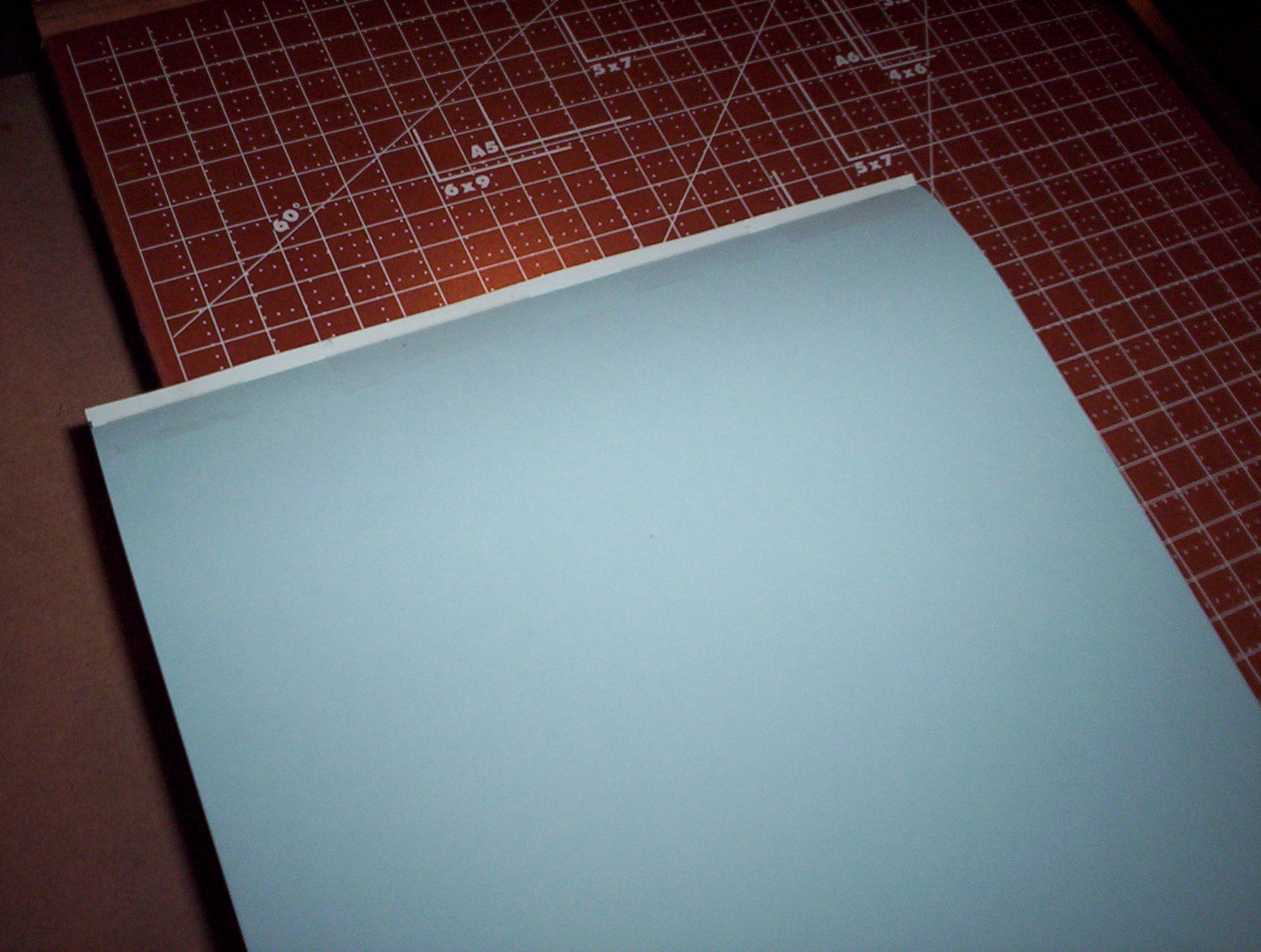
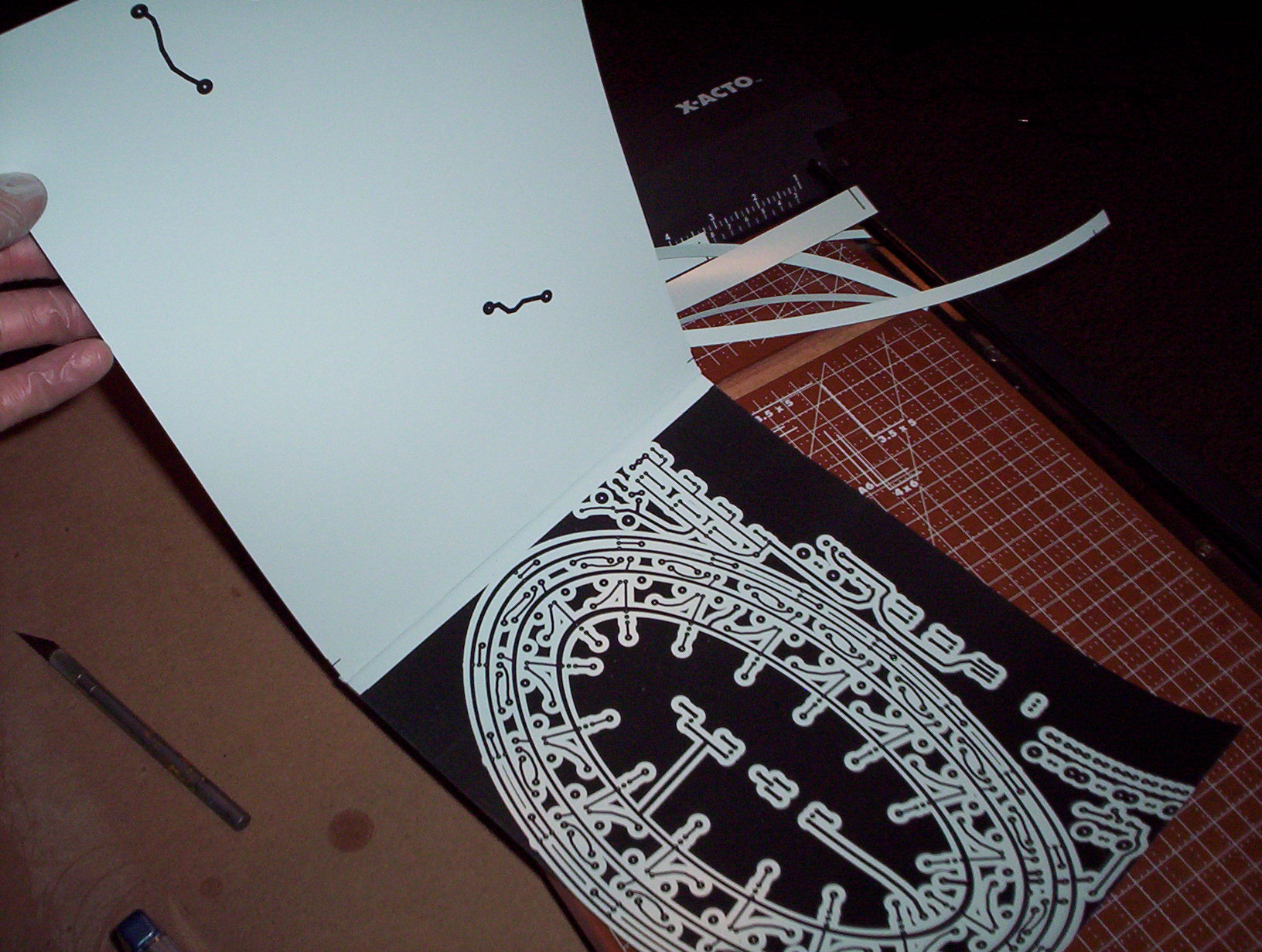
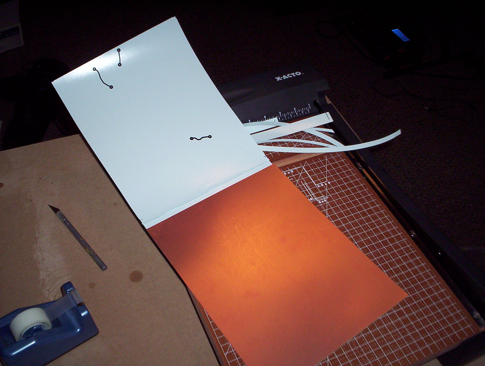
In order to keep everything lined up for the 2-sided PCB, I printed registration marks along with the PCB design. I trim the edges off along the registration marks. I leave one side uncut to provide some room to fit the board in between them without bending the paper. I then line up the two pages facing each other and tape them together along the uncut edge.
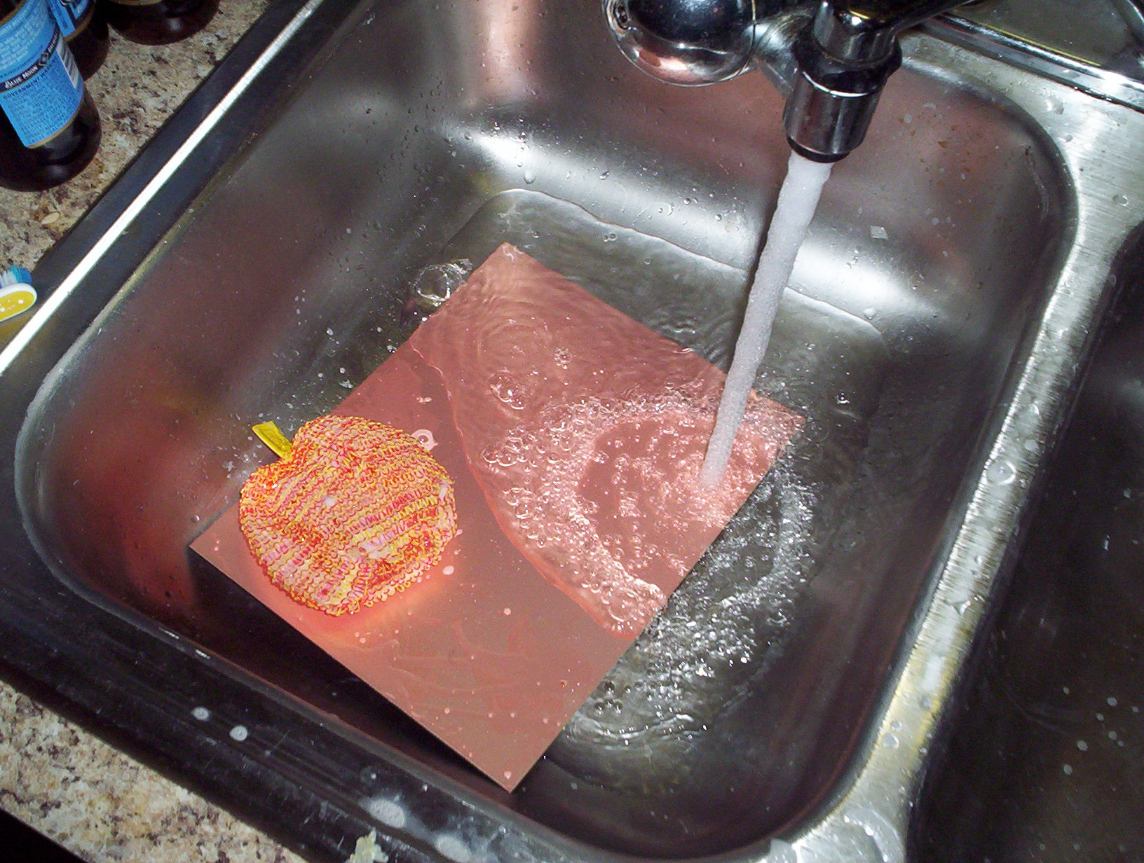
Now I clean the copper clad board. I just use some soap and water and a non-abrasive plastic scrubby. This removes any dirt or protective layer that would interfere with the etching process. Dry it really good!
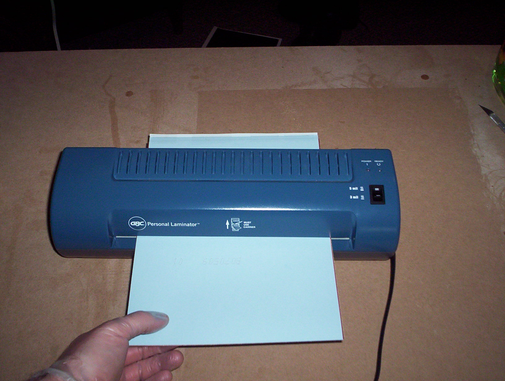
I sandwich the board between the toner transfer papers and run it through my GBC Personal Laminator. This is seriously the best $60 I've ever spent. The key ingredients for a good toner transfer PCB are heat and pressure. You can use a common iron to do this, but in my experience it can be a frustrating process if you do not have patience. Keeping a uniform and evenly distributed pressure with an iron requires some practice. And it's especially difficult on larger boards such as this. The laminator makes this much easier because you just feed it through for an even distribution of heat and pressure. The only trick with this device is thick PCBs are difficult to get through. Luckily, I've got a good source of surplus thin copper clad boards from Electronic Goldmine. I run this board through the laminator many times; maybe 2 dozen times. This is probably overkill, but it beats having to start over if I didn't run it through enough times.
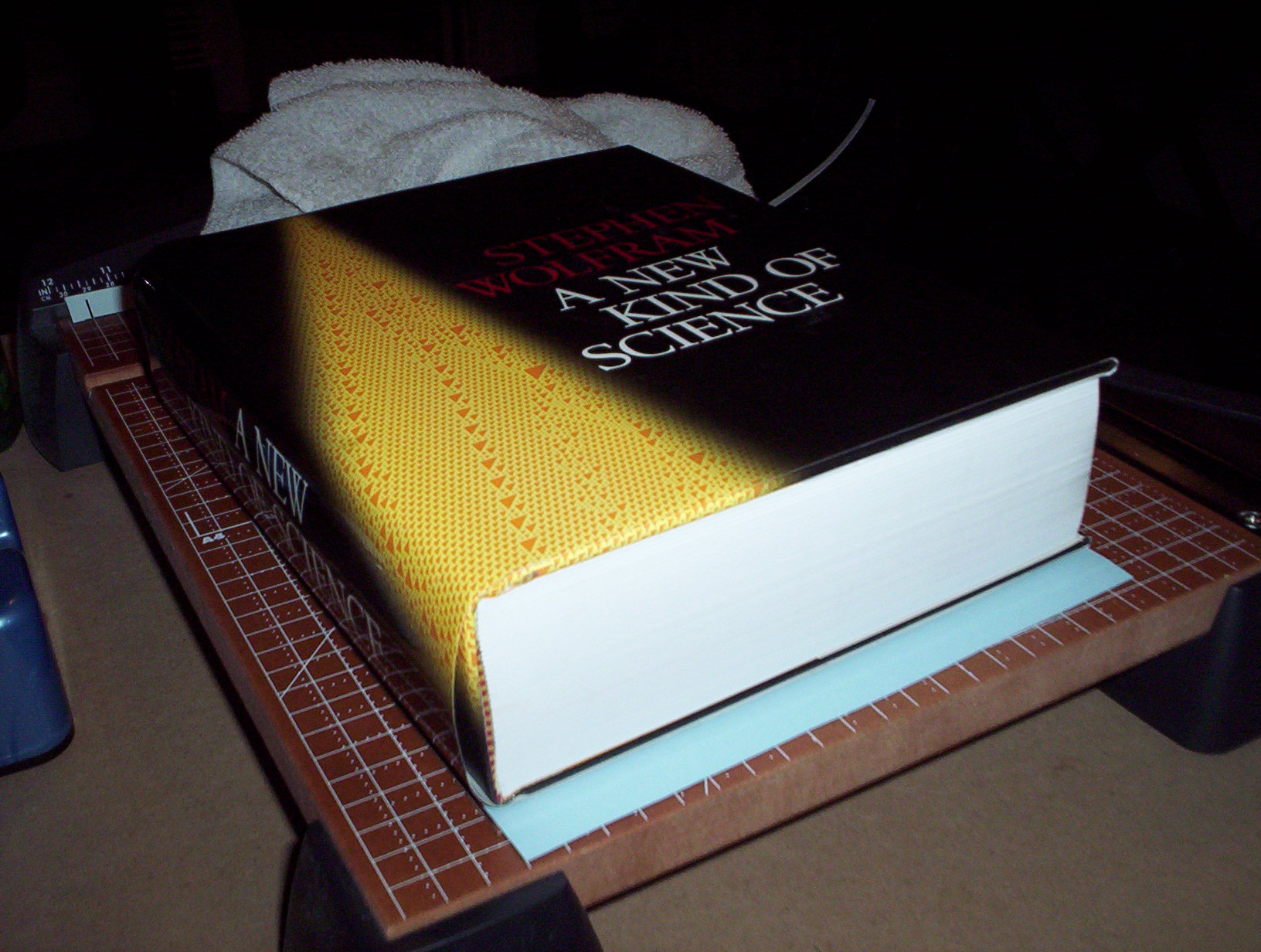
When I'm done feeding it through, I put a big heavy book on top of the board to keep some pressure on it while it cools off.
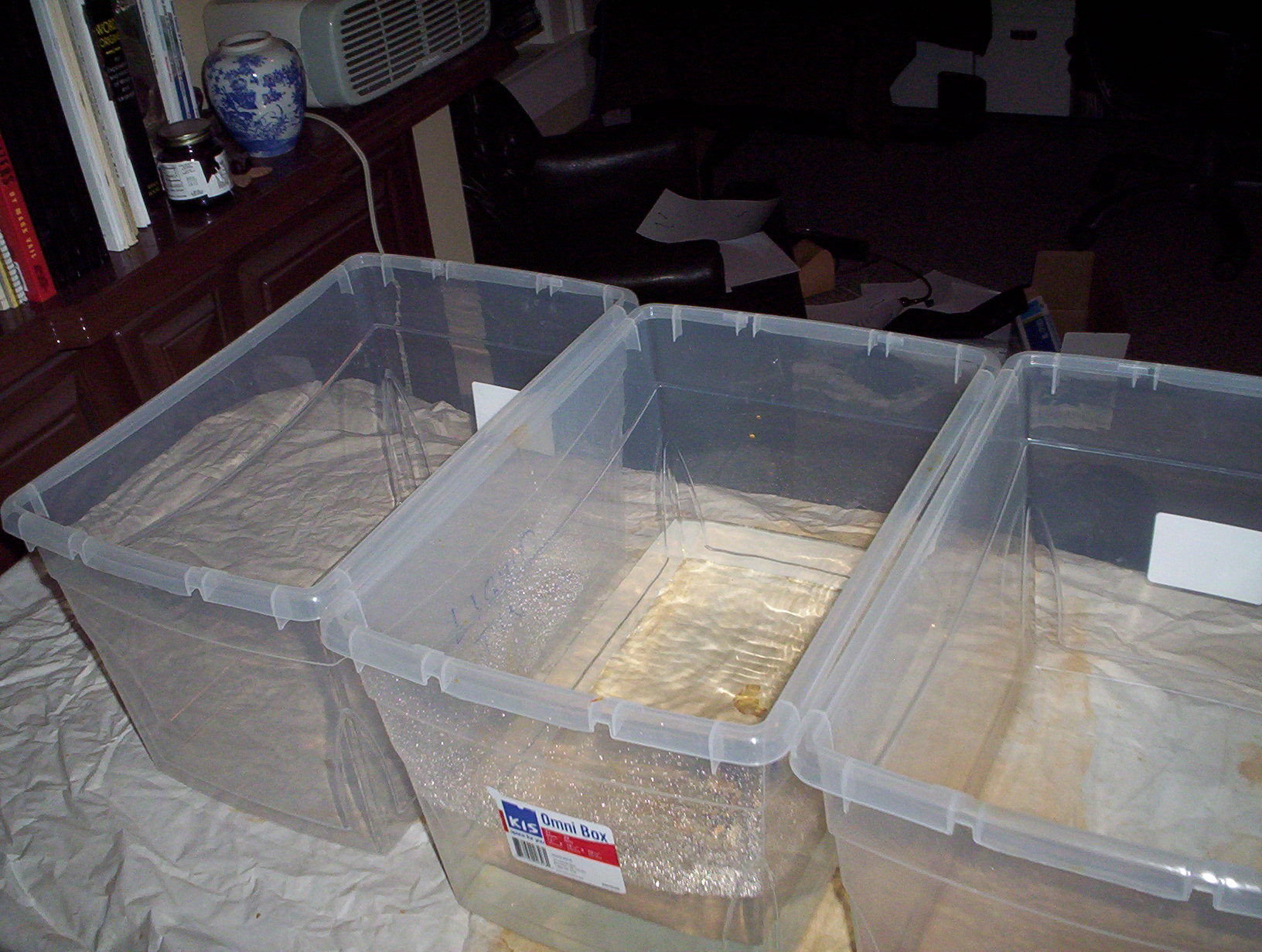
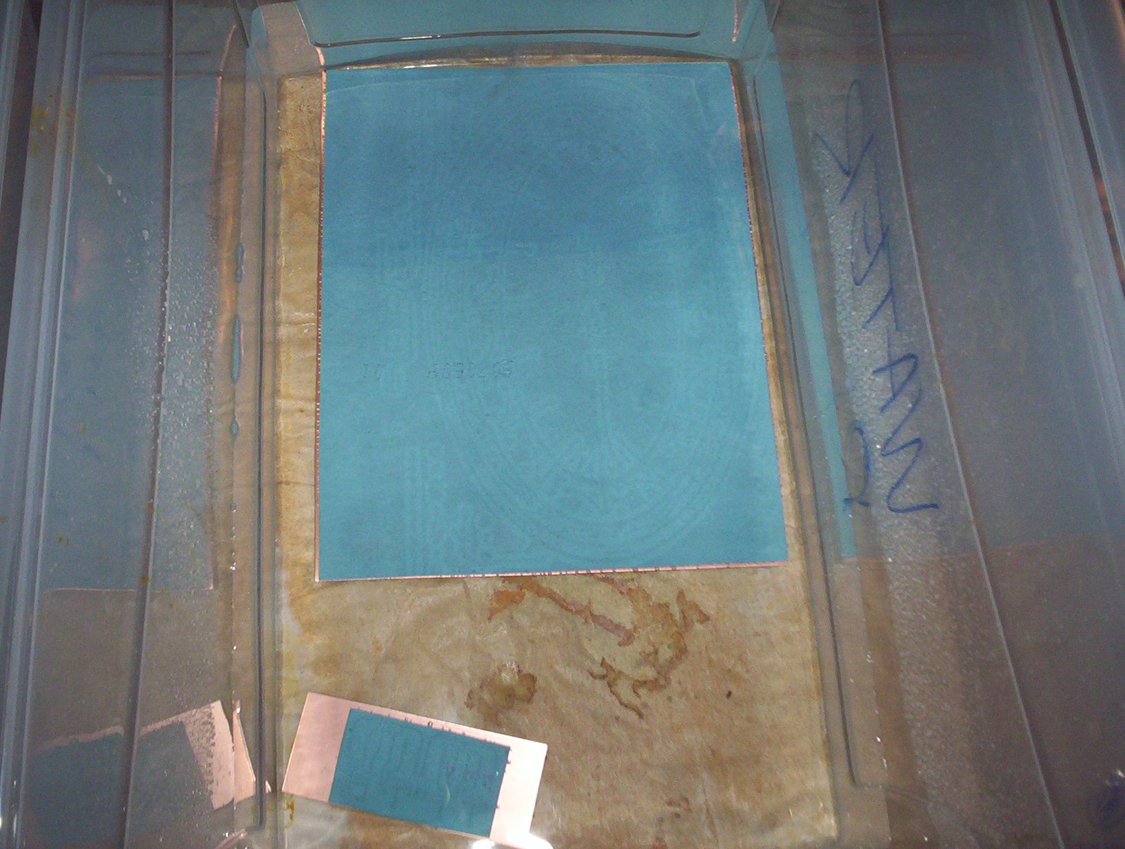
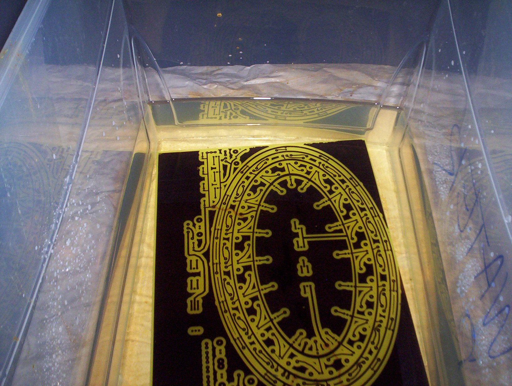
Set up some tanks for water, etchant and liquid tin (optional). I'm using some big plastic tubs because of the size of the board I'm making. Big tubs are better because there's less chance of stuff splashing out while you are agitating the board. I submerge the PCBs. Within a couple of minutes the toner transfer sheet will lift off by itself. You will be left with the laser printer toner fused to the PCB.
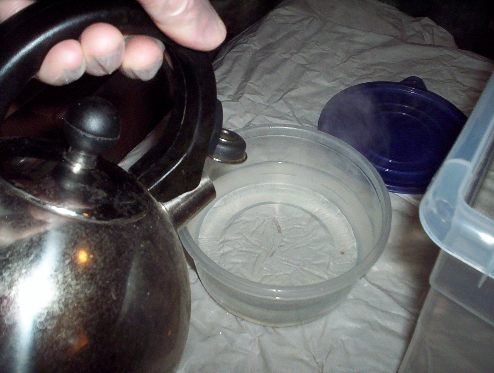
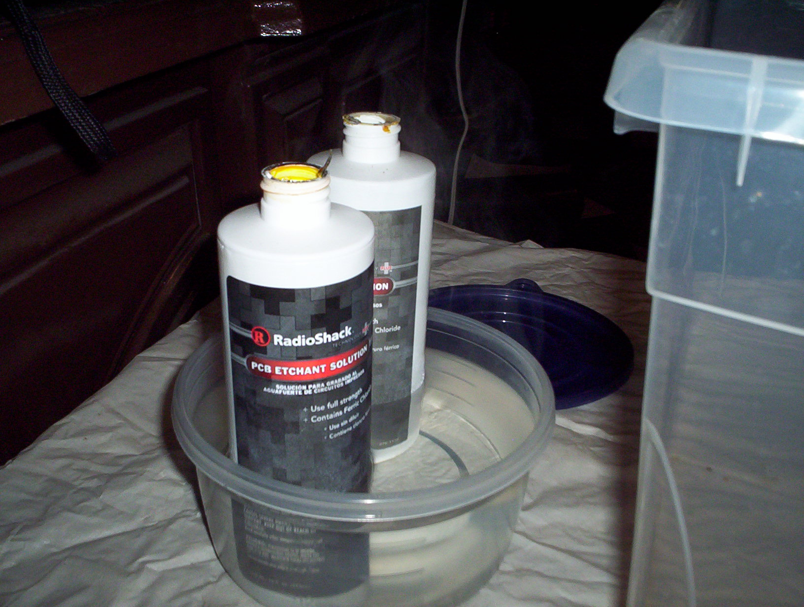
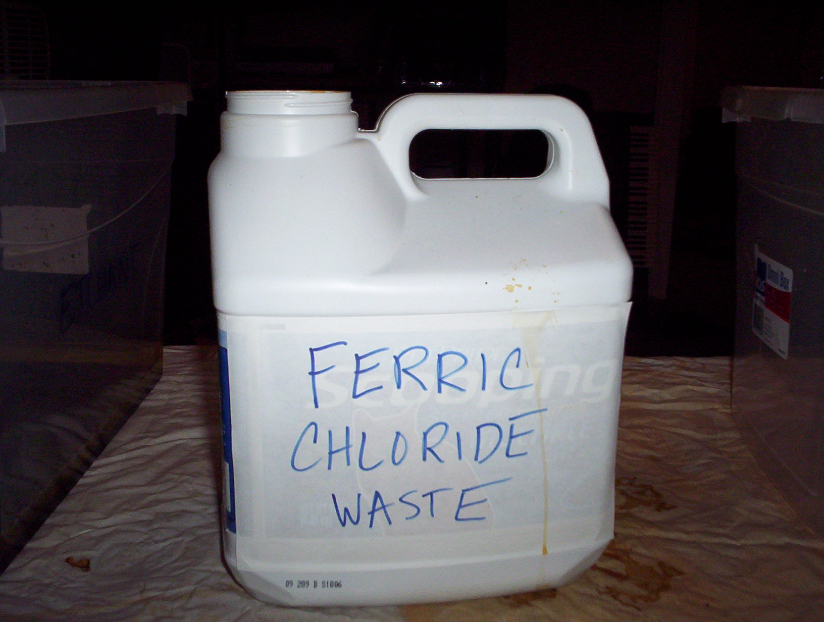
Now I'm preparing the etchant. This is what will eat away all the exposed copper, leaving the copper covered by the toner intact. I'm using ferric chloride. Believe it or not Radioshack carries this again. It used to be I had to find the oldest Radioshack in town and find their back stock.. Ferric chloride will stain anything it touches so be careful. Do not let it come in contact with metal containers or metal pipes. It's like the blood in Aliens and will gradually eat through anything metal. Always use plastic containers and keep your waste for proper disposal at a hazardous waste center near you. Always read and follow safety instructions when handling hazardous chemicals. There are other etchant options besides ferric chloride that are a little cleaner, but I'll save that for another post. I warm up the ferric chloride by setting it in a bath of hot water. Heat and agitation speeds up the etching process.
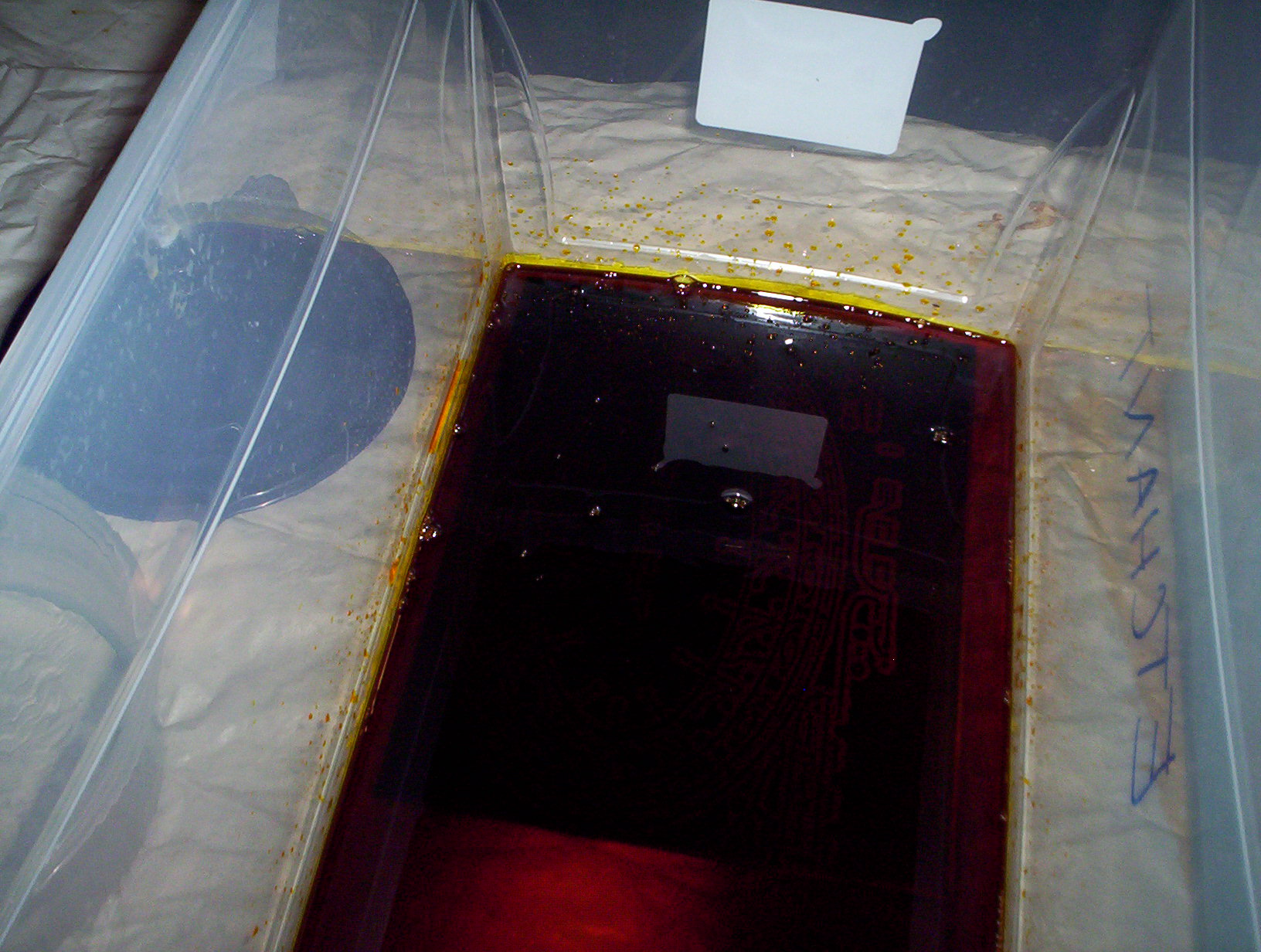
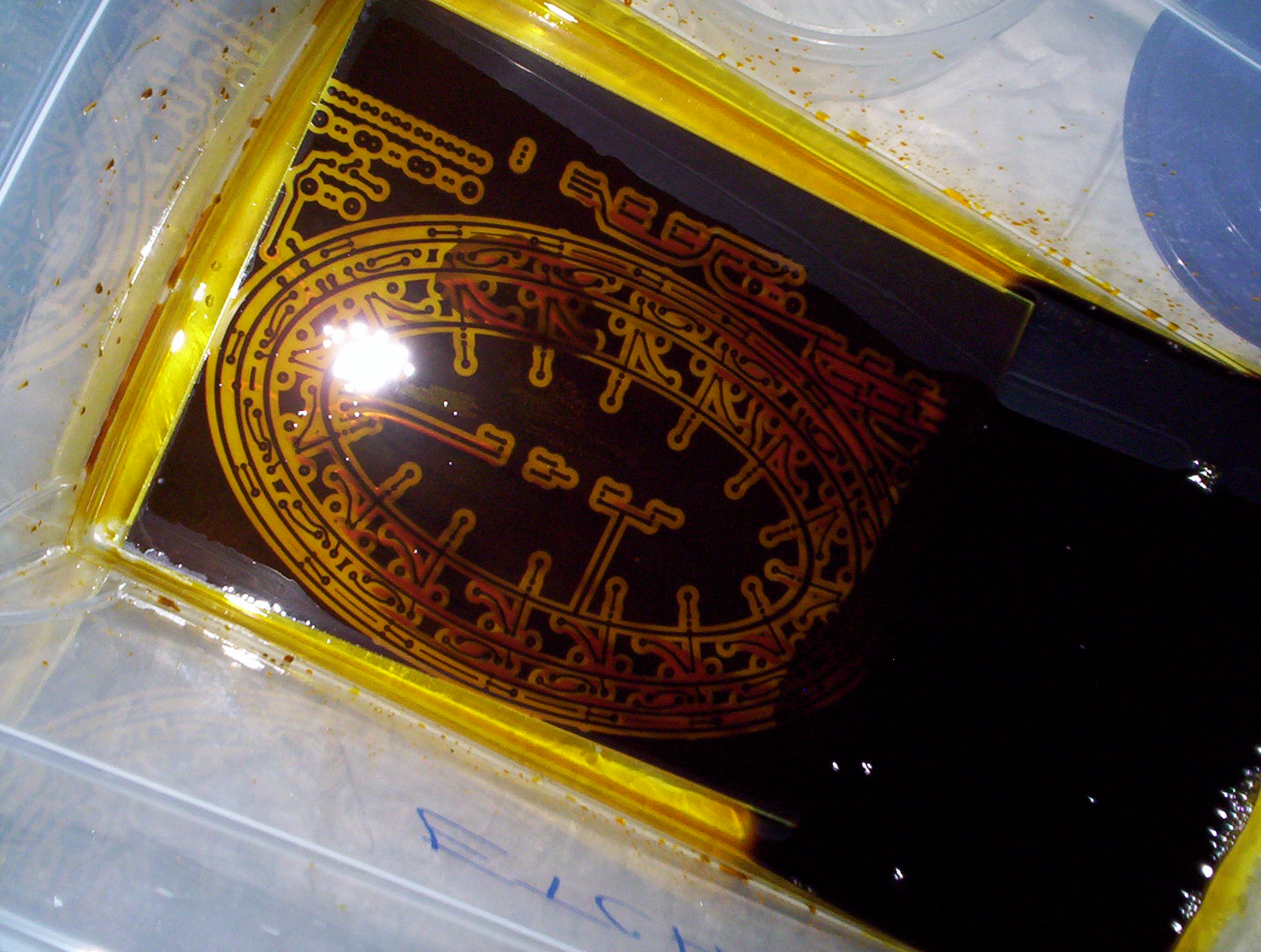
Drop the PCB in the tank and agitate it. Basically just rock the container back and forth to keep the solution flowing over it.
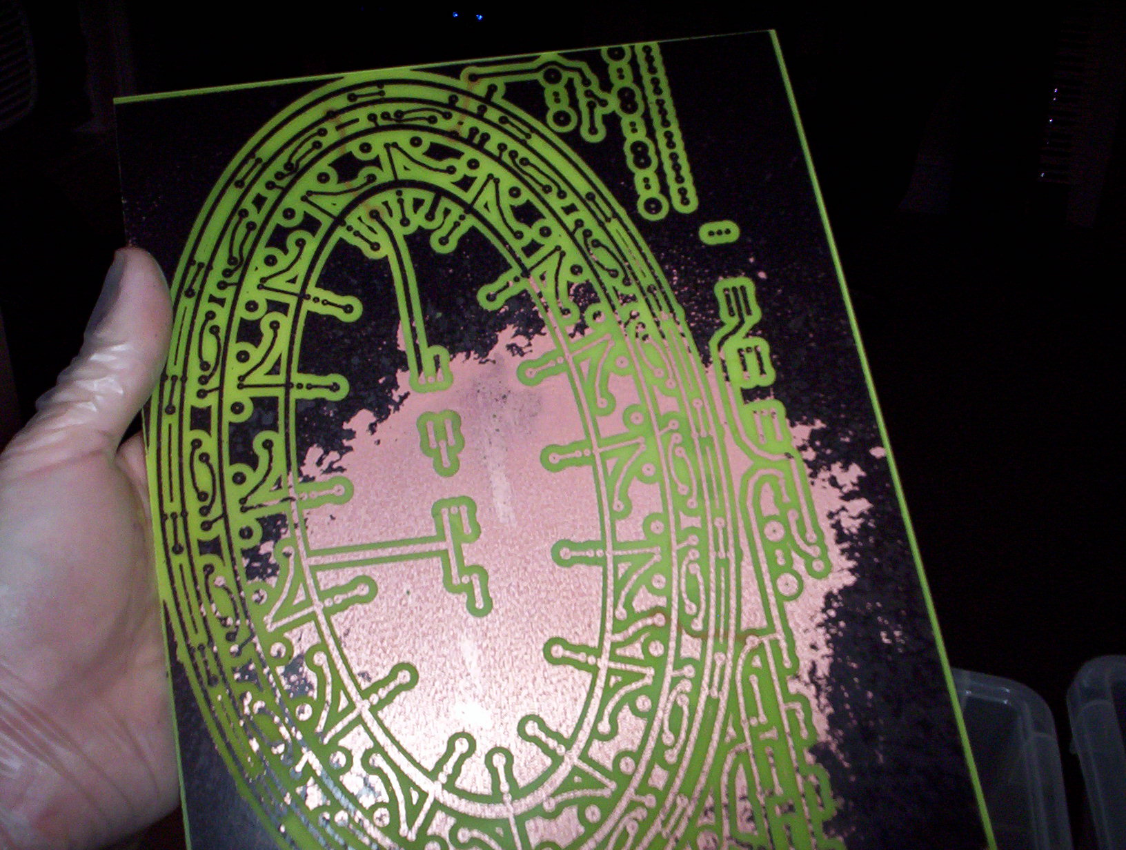
When the fiberglass PCB shows through and all the copper has been etched away move the PCB to a cold water bath. This will stop the etchant reaction. You are wearing rubber gloves right?
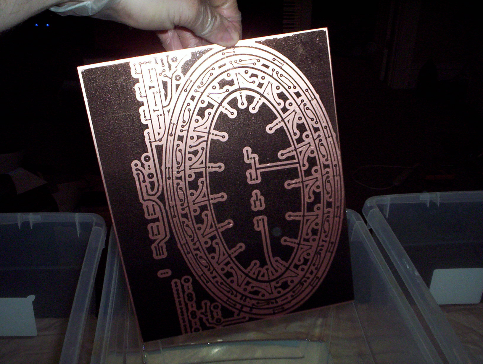
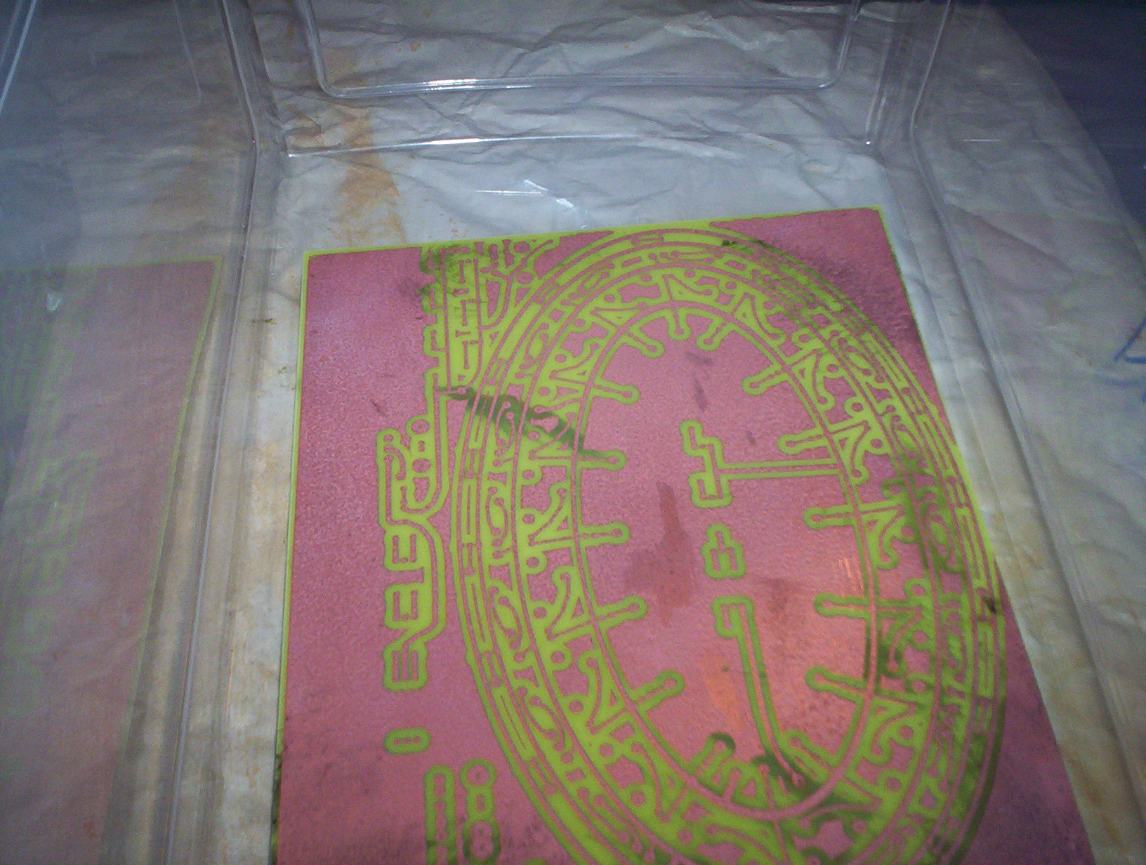
Now I use some nail polish remover and a cloth to remove the toner. The best stuff to use is Acetone nail polish remover from a pharmacy that's professional grade. 100% acetone. You're left with the copper traces from your PCB artwork!
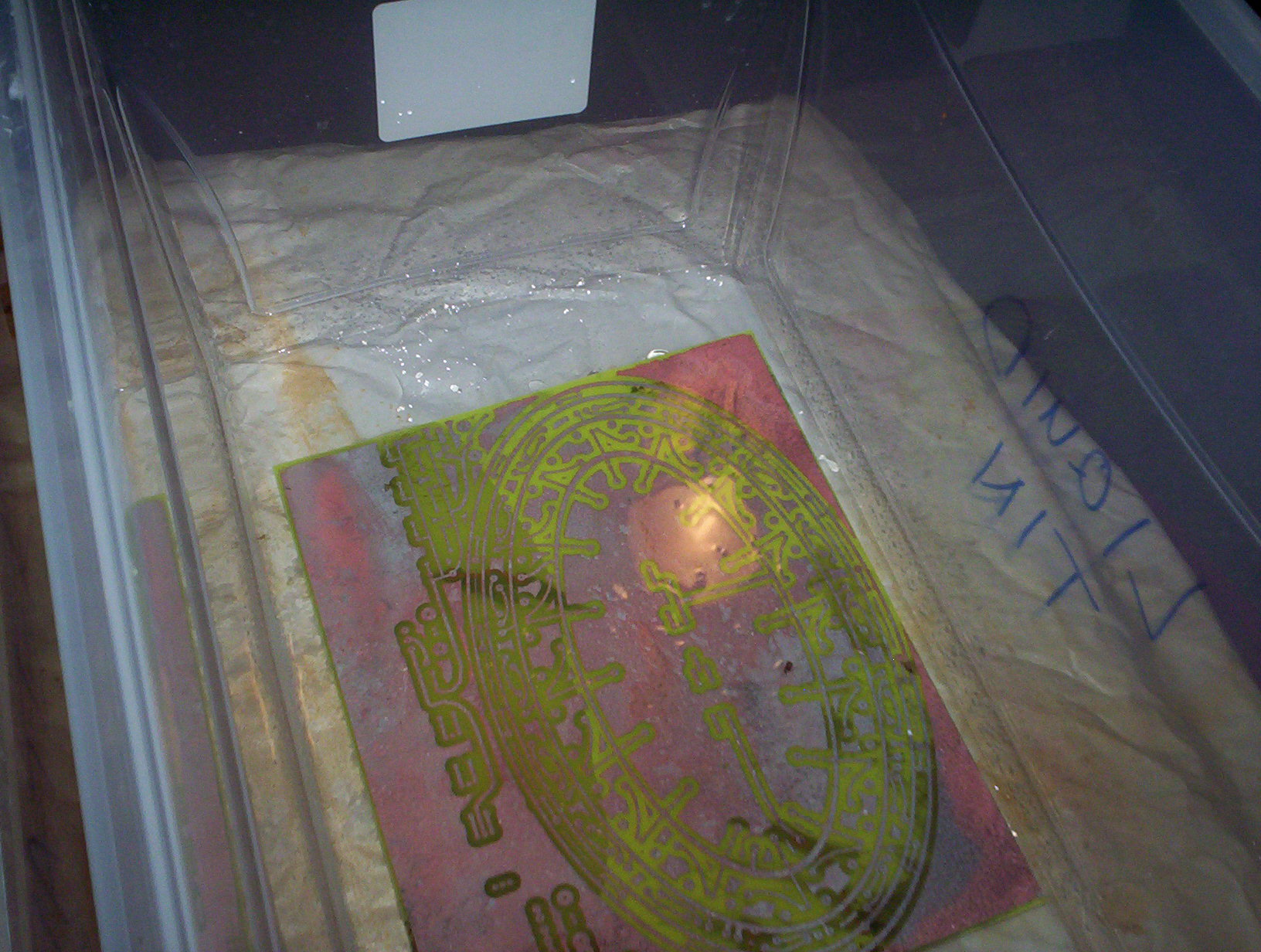
This step is optional. I use a solution called Liquid Tin to tinplate the copper and prevent future corrosion. Be careful with this stuff! It's a known carcinogen and can cause all types of ghastly cancers. Again follow ALL safety instructions!
Last step is to drill out the holes for the PCB, but I'll save that for the next post. Remember to properly contain your waste chemicals! I keep a plastic container that I can take to a hazardous waste disposal facility at some point in the future.
This particularly PCB fiberglass tended to soak up some of the toner during the removal process. It looks a little dirty, but it will function as necessary.






Good walkthrough Chris. I have always used Acetone to remove the toner also but I have seen this video that shows you can just scrub it off without hurting the board. http://www.youtube.com/watch?v=T5-laJBNNuw#t=5m56s . Like you said it will not will not keep it from working or anyways but if you are worried about the looks it may be something to keep in mind.
True. Acetone just works so fast though!
Good Detail. Thanks for posting such great pictures of each step in the process.
hi chris good work.
but i have some difficulties.......
HERE IN INDIA I COULD NOT GET LIQUID TIN VERY EASILY SO IS THERE ANY OTHER OPTION AVALIABLE FOR LIQUID TIN?? AND WHAT HAPPEN IF I MAKE PCB WITHPUT LIQUID TIN??
EAGERLY WAITING FOR YOUR REPLY
paranjape.aj@gmail.com
Thanks Anand. LIQUID TIN IS USEFUL FOR PREVENTING LONG TERM CORROSION, BUT IT IS NOT CRITICAL. YOU CAN SKIP LIQUID TIN APPLICATION ENTIRELY IF IT'S NOT AVAILABLE TO YOU.
Hi
How thick copper sheet can get through this laminator? Can I use 0,9mm sheet?
Could you please send me answer to my e-mail.
rudolfmolnar7@gmail.com
Thank you
It depends on the brand of laminator, but the one listed here will accept up to a 1mm thickness.