I'm working on a new synthesizer module for my rig called a 'Klee' sequencer. I'll detail more throughout the build process, but I want to share my experience using Inkscape to design a front panel.
Inkscape is great! It's an open source, cross platform vector graphics program with many uses. I started playing around with it a couple of years ago to create show fliers. I'm by no means proficient, but I know how to get around.
Back to the panel... I'm trying to cram lots of potentiometers, jacks and LEDs into a smaller panel in order to save space. I found some Alpha clear-shaft potentiometers that you can position a 3mm LED underneath. Very cool, although I have yet to find clear acrylic knobs to match.. In addition, I want to layout the sequencer lights in an oval pattern. Normally I'd use gEDA's pcb program to do a circuit design. But my components are very uniform and the layout is straightforward so I'll draw it up in... inkscape!
First I can use the datasheets for my components to get precise dimensions. Inkscape allows you to create shapes with precise units in px, mm, inches, etc. I make the footprints for each component and they look like this.

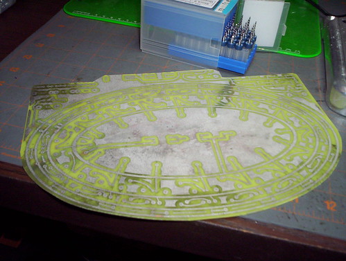
The blue circles are guides for drilling holes in the panels. The red shapes show how large the components are. The black circles are via pads for a solder mask. I copy, move, rotate all of these elements to fit everything into my panel layout. Then I draw traces between these pads for the PCB layout. I can also label them so I remember what's what. I'll come back to this with a more detailed process at some point, but here's the final drawing after all of that.

Click on the image for the full size awesomeness. Next I can separate all the colors into different layers with Inkscape's XML editor. Here's what I'll use to etch the PCB bottom layer.

There's also a top layer, but we can skip that. Here's the drill layer template I'll use to drill out all the panel holes.

That's all for now. Next in this series, I'll show you how I prepare and etch the PCB. Inkscape rules, it's good for lots of things beyond making web graphics.