
I ordered the parts  we'll need to do the first 5 experiments. I bought everything from Jameco. Here is the list of part numbers I used in case anyone is interested. We'll start work next week.
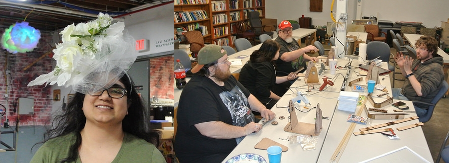
Solder your own Freeduino Feb. 27th
UPDATE: SOLD OUT on Feb. 14th.
ONE TICKET LEFT AT THE TIME OF THIS POST!

If it's sold out and you want to attend, never fear there will be more coming soon! These workshops are proving to be very successful and we'll keep doing them as long as there's interest. Keep watching the calendar on this blog and the Google Group for more info!
Using Inkscape for front panel layouts and PCBs
I'm working on a new synthesizer module for my rig called a 'Klee' sequencer. I'll detail more throughout the build process, but I want to share my experience using Inkscape to design a front panel.
Inkscape is great! It's an open source, cross platform vector graphics program with many uses. I started playing around with it a couple of years ago to create show fliers. I'm by no means proficient, but I know how to get around.
Back to the panel... I'm trying to cram lots of potentiometers, jacks and LEDs into a smaller panel in order to save space. I found some Alpha clear-shaft potentiometers that you can position a 3mm LED underneath. Very cool, although I have yet to find clear acrylic knobs to match.. In addition, I want to layout the sequencer lights in an oval pattern. Normally I'd use gEDA's pcb program to do a circuit design. But my components are very uniform and the layout is straightforward so I'll draw it up in... inkscape!
First I can use the datasheets for my components to get precise dimensions. Inkscape allows you to create shapes with precise units in px, mm, inches, etc. I make the footprints for each component and they look like this.

The blue circles are guides for drilling holes in the panels. The red shapes show how large the components are. The black circles are via pads for a solder mask. I copy, move, rotate all of these elements to fit everything into my panel layout. Then I draw traces between these pads for the PCB layout. I can also label them so I remember what's what. I'll come back to this with a more detailed process at some point, but here's the final drawing after all of that.

Click on the image for the full size awesomeness. Next I can separate all the colors into different layers with Inkscape's XML editor. Here's what I'll use to etch the PCB bottom layer.

There's also a top layer, but we can skip that. Here's the drill layer template I'll use to drill out all the panel holes.

That's all for now. Next in this series, I'll show you how I prepare and etch the PCB. Inkscape rules, it's good for lots of things beyond making web graphics.
Using Make: Electronics in my classroom
I teach high school physics at Kentucky Country Day School. All of our freshman take physics, but there isn't time to cover all the topics one would like. For this reason I also teach Physics II. It is taken mainly by seniors who want to learn about some of the topics that were omitted from the freshman class. Physics II is a conceptual physics course. Qualitative understanding is emphasized over calculation and I try to help the students develop their physics intuition through exercises like one might find in the book Thinking Physics. This year I decided to spend several weeks using the new Make: Electronics book. It takes the same approach of doing first to develop understanding over calculating starting with theory. The fact that it is totally hands on will appeal to my students, especially when senioritis starts to set in. Â I plan to post updates here about how it's going and to share what I learn from the experience. Keep checking back if you are interested.