Skip to content

About Christopher

Micro Colonel of LVL1

7

This is continued from my previous post about using Inkscape to draw pcb and front panel designs. When I last left you, I had created a multi-layered inkscape drawing that had front and back designs for the PCB along with a drill pattern for the panel.

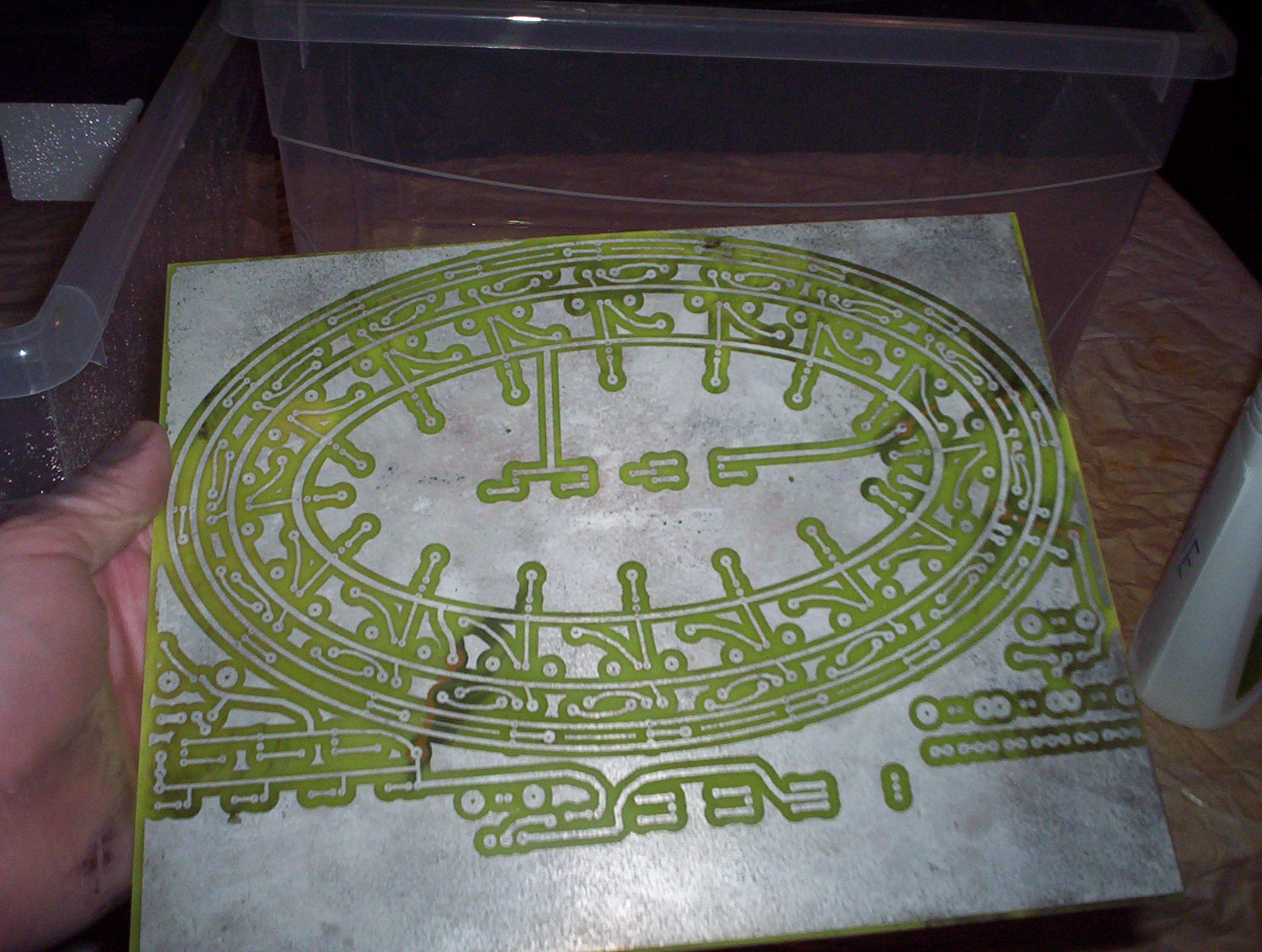
First I'm going to get out my Toner Transfer paper. This is thick stock paper with a water soluble coating. It allows you to fuse a printed image to a surface and then remove the paper when submerged in water. The stuff is a little pricey at about $1 a page, but it's well worth it for making good clean transfers.

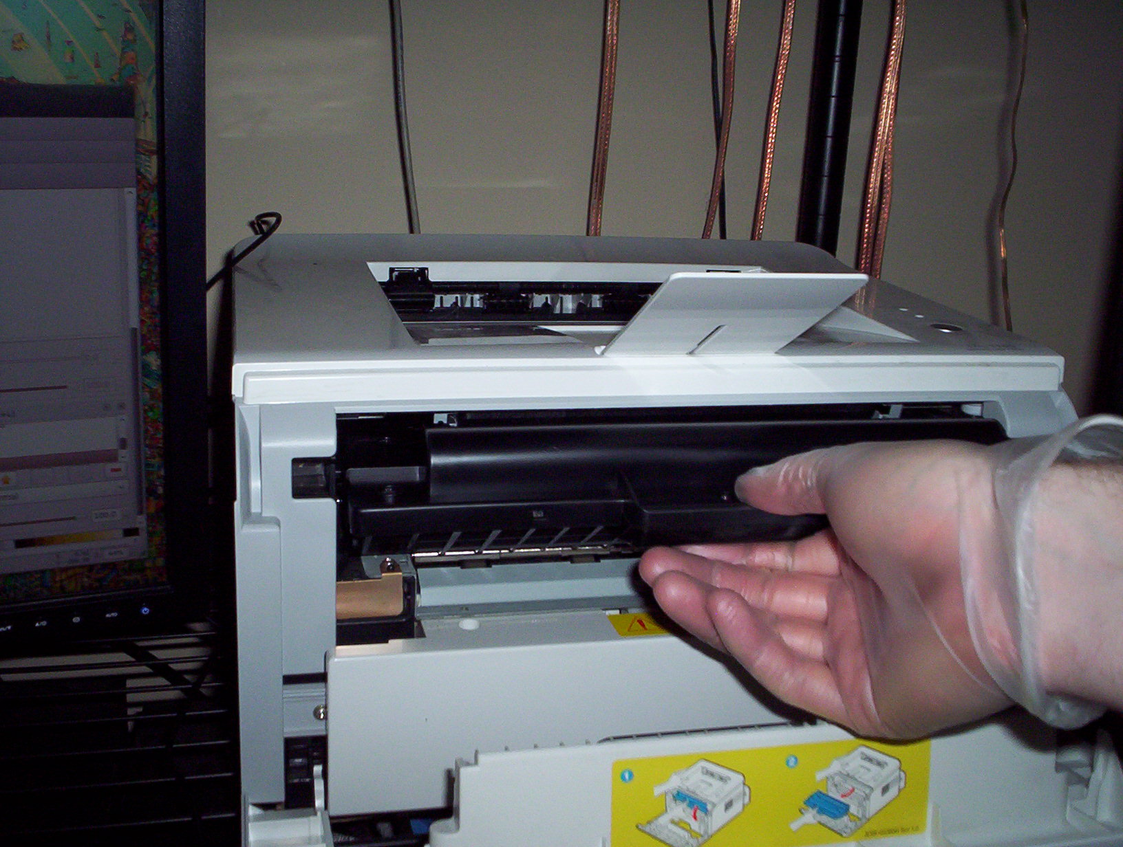
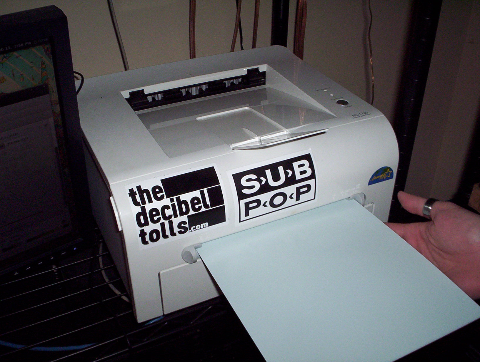
I'm using my home laser printer to make the PCB transfer. Ink from a laser printer is fused to the paper when heat and pressure is applied. Note that an inkjet printer uses a different method not suitable for the process I'm describing here. LASER PRINTERS ONLY. I keep a spare laser printer cartridge that I use solely for making PCBs. It's best to have a dark layer of ink. Regular printing jobs will run down the cartridge and I do this often enough that it makes sense to have a separate cartidge.

I start the print job and manually feed the Toner Transfer paper. Make sure you're printing on the shiny reflective side!

...continue reading "Creating Custom PCBs for a Front Panel"

UPDATE: SOLD OUT on Feb. 14th.

ONE TICKET LEFT AT THE TIME OF THIS POST!

If it's sold out and you want to attend, never fear there will be more coming soon! These workshops are proving to be very successful and we'll keep doing them as long as there's interest. Keep watching the calendar on this blog and the Google Group for more info!

1

I'm working on a new synthesizer module for my rig called a 'Klee' sequencer. I'll detail more throughout the build process, but I want to share my experience using Inkscape to design a front panel.

Inkscape is great! It's an open source, cross platform vector graphics program with many uses. I started playing around with it a couple of years ago to create show fliers. I'm by no means proficient, but I know how to get around.

Back to the panel... I'm trying to cram lots of potentiometers, jacks and LEDs into a smaller panel in order to save space. I found some Alpha clear-shaft potentiometers that you can position a 3mm LED underneath. Very cool, although I have yet to find clear acrylic knobs to match.. In addition, I want to layout the sequencer lights in an oval pattern. Normally I'd use gEDA's pcb program to do a circuit design. But my components are very uniform and the layout is straightforward so I'll draw it up in... inkscape!

First I can use the datasheets for my components to get precise dimensions. Inkscape allows you to create shapes with precise units in px, mm, inches, etc. I make the footprints for each component and they look like this.

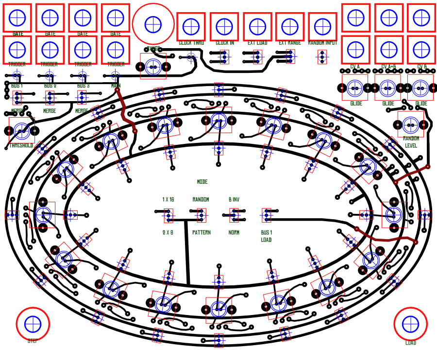
The blue circles are guides for drilling holes in the panels. The red shapes show how large the components are. The black circles are via pads for a solder mask. I copy, move, rotate all of these elements to fit everything into my panel layout. Then I draw traces between these pads for the PCB layout. I can also label them so I remember what's what. I'll come back to this with a more detailed process at some point, but here's the final drawing after all of that.

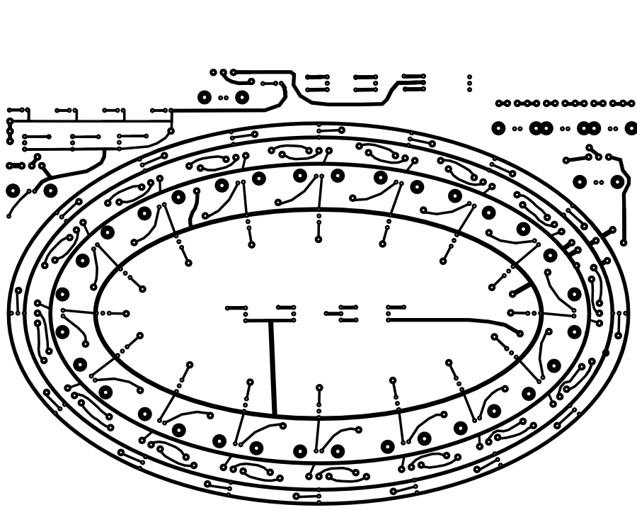
Click on the image for the full size awesomeness. Next I can separate all the colors into different layers with Inkscape's XML editor. Here's what I'll use to etch the PCB bottom layer.

There's also a top layer, but we can skip that. Here's the drill layer template I'll use to drill out all the panel holes.

That's all for now. Next in this series, I'll show you how I prepare and etch the PCB. Inkscape rules, it's good for lots of things beyond making web graphics.